Packaging equipment by application
Pick your process. Each note explains the hard part, how ENG equipment handles it, and which machines to evaluate.
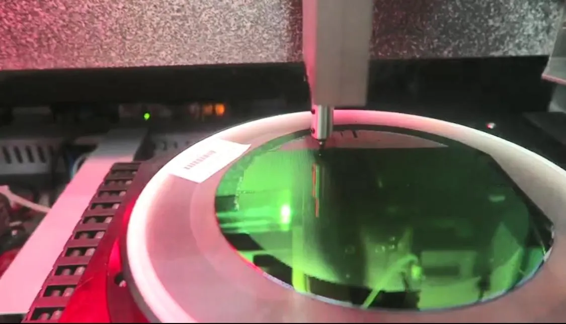
Optical module die bonders for 800G and 1.6T transceivers
Place VCSEL, PD, MPD, TIA and COC die to ±3 μm @3σ, and passive parts, isolators, windows, FA, with UV cure in the same line.
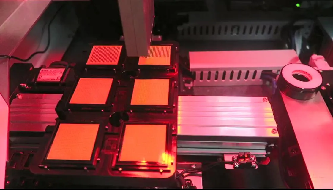
Eutectic die bonder for EML, LD and COC laser chips
EX20 forms an atomic-level eutectic bond with ±1.5 μm @3σ placement, two alternating heating stations and fully programmable multi-stage profiles.
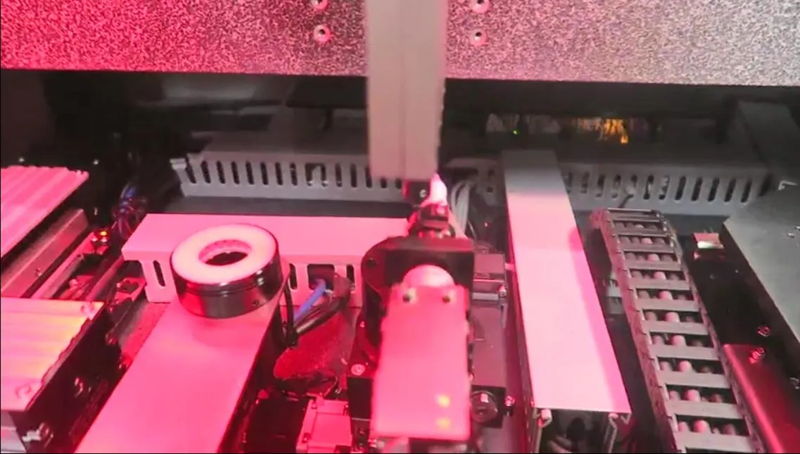
Automatic active alignment for silicon photonics and CPO optical engines
C20 couples single or dual lenses to 50-100 nm with ≤±0.3 μm XY, real-time optical power feedback and full data traceability.
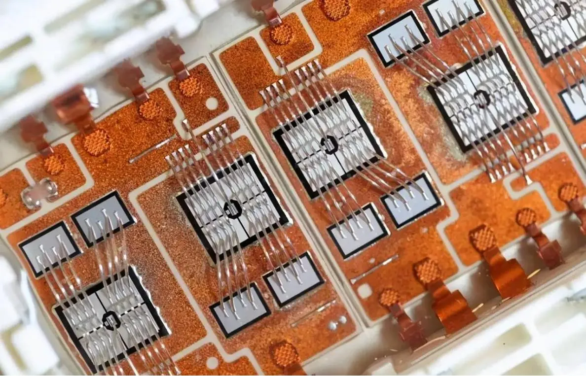
SiC sintering die attach and IGBT / IPM module assembly
Silver-paste and silver-film pre-sintering for SiC, six-head multi-chip bonding for IGBT and IPM, and one-machine module assembly.
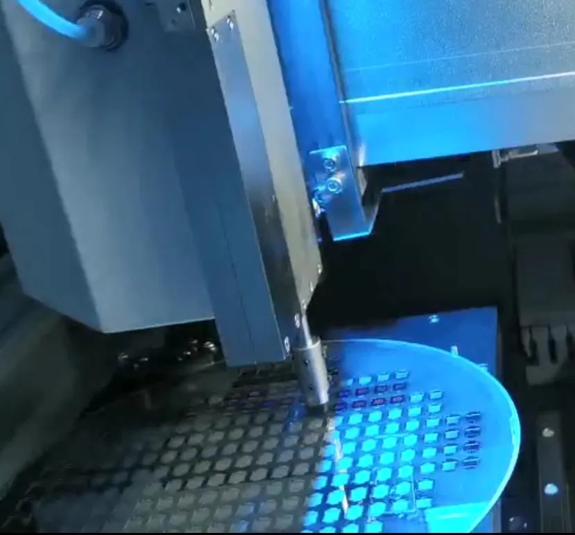
MEMS and sensor die bonding with membrane-safe handling
Pick and place fragile MEMS die without touching the membrane, then wedge-bond with Al or Au wire.
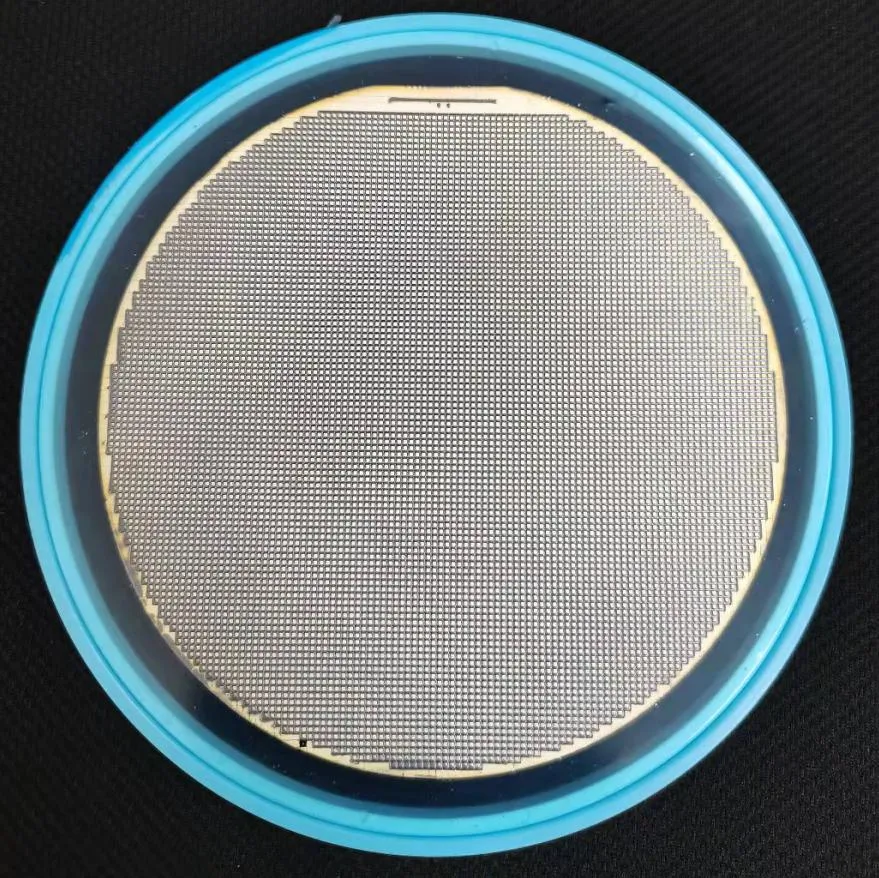
High-throughput flip chip bonder for FCBGA, FCCSP and FC QFN
A19 FC: 12 bond heads on two gantries, ±5 μm @3σ global accuracy, up to 10,000 UPH.
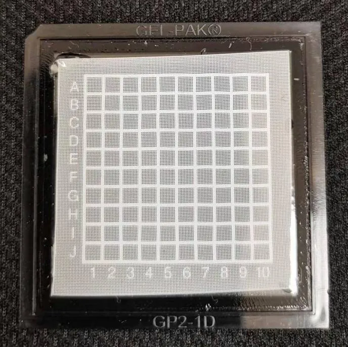
Die sorter for optical, power and MEMS die
S17 sorts, flips and transfers die from 0.2 mm to 16 mm at up to 7,000 UPH.
Send us your die. We'll bond it.
Free sample bonding on the matching ENG machine. Share die, substrate and accuracy target, and an engineer replies within 24 hours.
- SendDie, substrate and target accuracy, under NDA if needed
- BondENG engineers run your parts on the matching machine
- ReportPlacement accuracy, process notes and a machine recommendation