Flip Chip Bonder
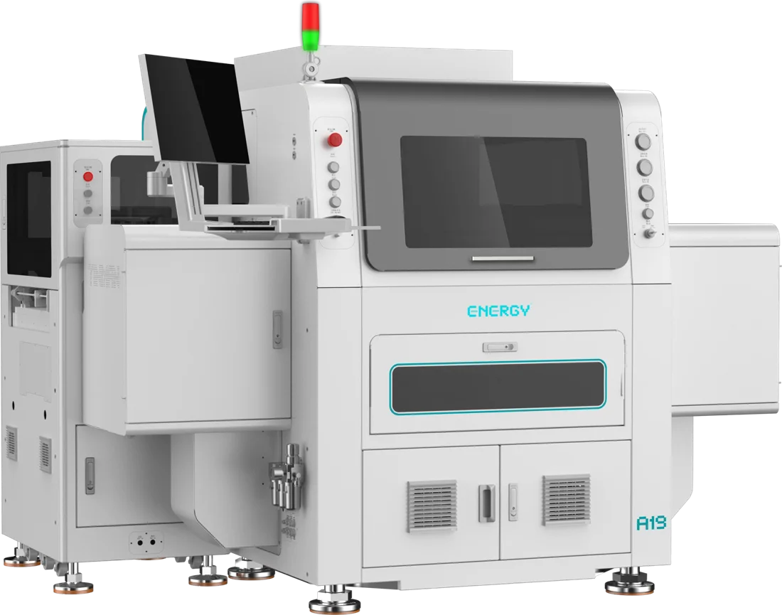
A19 FC
Up to 10,000 UPH @ 5 μm with a patented 12-head, dual-gantry design
- XYθ global @3σ
- ±5 μm
- Max UPH (no dip)
- 10,000
- Bond heads
- 12
- Wafer
- 8/12 in
What it does
A19 FC is a high-throughput flip chip bonder. Each gantry picks 6 die at once and two gantries run in parallel; dipping is integrated. SECS/GEM, SMEMA and TCP/IP interfaces fit it into an automated line.
Suitable for
- FCPGA, FCCSP and FCBGA
- FC SOT, FC LGA and FC QFN
- FR4/FR5, BGA, lead frame, MIS and ceramic substrates
Highlights
- ±5 μm @3σ and ±0.05° @3σ global placement
- Max 8,000 UPH with dipping, 10,000 UPH without, at 5 μm
- Open/closed-loop bond force 50-3,000 g
- Class 1,000 (ISO 6) cleanliness
- Optional AOI pre-scan module, ±3 μm @3σ
A19 FC specifications
Manufacturer data, H1 2026. Throughput is under the stated standard conditions. Final values are confirmed in the technical agreement for your process.
| XYθ global placement accuracy | ±5 μm @3σ, ±0.05° @3σ |
|---|---|
| Throughput (with dipping) | Max 8,000 @ 5 μm |
| Throughput (no dipping) | Max 10,000 @ 5 μm |
| Bond force | Open/closed loop 50-3,000 g (50-100 g ±5 g; 100-3,000 g ±5%) |
| Die size | 0.5×0.5-11×11 mm (max 30×30 optional) |
| Die thickness | 50-2,000 μm |
| Wafer cassette | Single; dual optional |
| Wafer size | 8/12 in |
| Wafer rotation | Automatic compensation |
| Ejector | Single or multi-needle, 6-needle library, automatic change |
| Bond heads | 6 per gantry, 12 total; 1 or 2 gantries optional |
| Nozzle change | Automatic |
| Flip / face-up | Flip; face-up optional |
| Transfer / buffer | Transfer and buffer module, 6 die per gantry at once |
| Dipping | Depth 20-200 μm configurable; viscosity 2,800-110,000 cps |
| Substrate size | L160-340 × W60-340 mm, thickness ≤6.0 mm |
| Substrate types | FR4/FR5, BGA, lead frame, MIS, ceramic |
| Substrate transfer | 3-section track, width 60-340 mm |
| Pre-scan | AOI pre-scan module (optional), ±3 μm @3σ |
| Magazine handling | Input/output magazines (optional) |
| Recognition | Fiducials (+, o, -, x, □), bad marks, bumps, edges |
| Cleanliness | Class 1,000 (ISO 6) |
| Calibration | Local / global automatic |
| Wafer mapping | SECS/GEM |
| Line interface | SMEMA |
| Network / protocol | TCP/IP, SECS/GEM |
| Cameras | Bond head (down-look) 5 MP, 9.1×7.4 mm FOV; bottom (up-look) 25 MP, 16×16 mm FOV; wafer 2 MP, 6×6 to 31×31 mm FOV |
| Power | 3.5 kW (AC 220 V, 50/60 Hz) |
| Air | 0.5-0.7 MPa, 350 L/min; vacuum ≤-90 kPa, 250 L/min; dried and filtered |
| Footprint | 1,700 (L) × 1,690 (W) × 1,550 (H) mm (excl. monitor and tower light) |
| Weight | 2,600 kg (main unit) |
| Inspection | Ink-dot recognition, die-defect similarity recognition |
| Safety | Deionizer, light curtain at operator window |
| Access control | Operator / engineer permission levels; wafer map read & generate (optional) |
Often evaluated with
Test your die on the A19 FC.
Send die and substrate samples or drawings. ENG engineers run a sample bonding and report placement accuracy and process results, free of charge.
- SendDie, substrate and target accuracy, under NDA if needed
- BondENG engineers run your parts on the matching machine
- ReportPlacement accuracy, process notes and a machine recommendation