Die sorter for optical, power and MEMS die
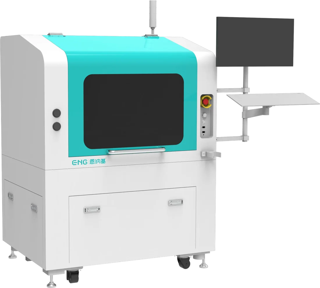
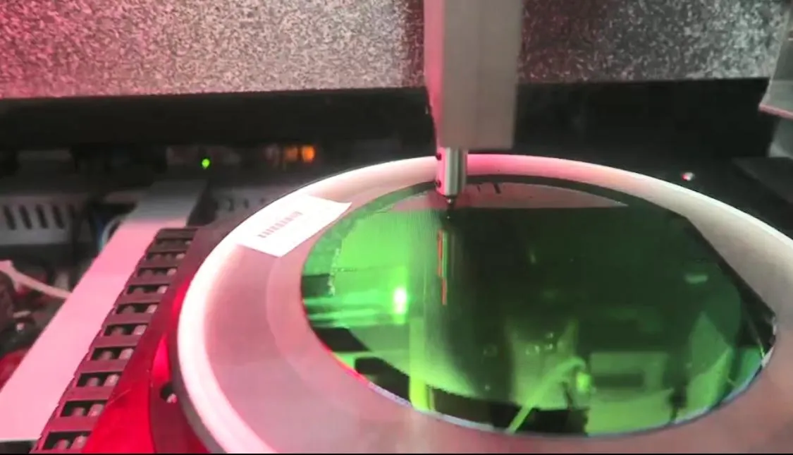
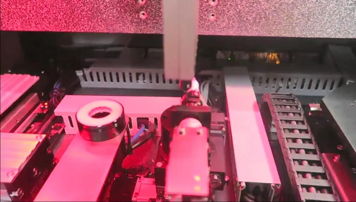
S17 sorts, flips and transfers die from 0.2 mm to 16 mm at up to 7,000 UPH.
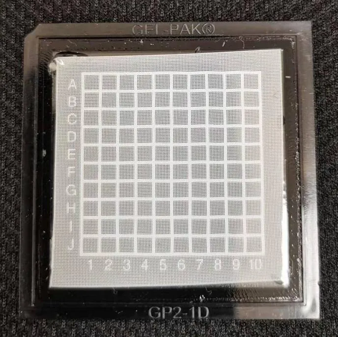
The hard part
Sorting sits upstream of every bond step. Fragile optical die, thin power die and coated MEMS die all need clean picks, the right flip and a wafer map that follows them.
How ENG equipment handles it
- Wafer-to-tray, wafer-to-wafer, tray-to-wafer.
- 0° / 90° / 180° flip; S17 Pro adds flip FC, bottom UL and pre-placement stage.
- ≥7,000 UPH (S17), best ±15 μm @3σ (S17 Pro).
- Wafer map read & generate (optional).
Machines to evaluate
Send us your die. We'll bond it.
Free sample bonding on the matching ENG machine. Share die, substrate and accuracy target, and an engineer replies within 24 hours.
- SendDie, substrate and target accuracy, under NDA if needed
- BondENG engineers run your parts on the matching machine
- ReportPlacement accuracy, process notes and a machine recommendation