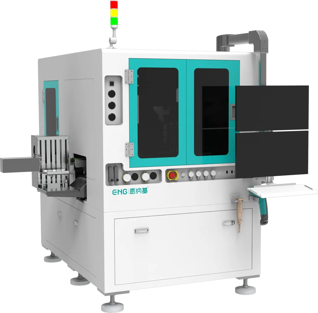
A laser chip is attached face down or face up to a submount, C-mount or carrier, and that one joint does two jobs. It carries heat away from an active region that can see very high heat flux, and it fixes the emitting facet to a mechanical edge that the next optical step depends on. Both jobs are set by the die bonder.
Facet overhang: the placement spec that matters
For high-power laser diode chip-on-submount builds, a published process note describes the key placement requirement as the position between the emitting front facet and the edge of the heat-sink substrate. Post-bond results should show no recess from the facet to the substrate edge, and facet overhang should be under 5 to 10 μm. The same note works backwards: if post-bond accuracy must be better than ±2.5 μm, and both the laser die and the submount edge carry up to 1 μm tolerance, then machine placement accuracy needs to be better than ±1.5 μm [1].
That is why the EX20 eutectic die bonder is specified at ±1.5 μm @3σ in XY and ±0.2° @3σ in angle. Ask any supplier how accuracy is measured: on a glass die, or on real parts after the solder freezes. The two numbers are not the same.
| Requirement | What the sources say | Process lever | EX20 data point |
|---|---|---|---|
| Facet position | No recess from the front facet to the submount edge, overhang under 5 to 10 μm [1] | Placement accuracy and angle control | ±1.5 μm @3σ XY, ±0.2° @3σ angle |
| Machine accuracy | Post-bond accuracy typically better than ±2.5 μm, so machine placement better than ±1.5 μm when parts hold under 1 μm tolerance [1] | Vision alignment on die and submount edge | ±1.5 μm @3σ XY |
| Voids | Voids and delamination can raise junction temperature sharply and end in failure [2] | Uniform heat, oxide control, uniform bond force | Dual heating stations, 10 × 10 mm area, ±5 ℃ |
| Solder contact area | Simulation matched tests at 85 to 90% interface contact for a single emitter [2] | Wetting quality and flat surfaces | Multi-stage profile, each stage set independently |
| Bond force | III-V die need programmed force per component type [1] | Closed-loop force by die size | Voice coil 20 to 50 g ±2 g, 50 to 300 g ±10% |
| Cycle time | A typical chip-on-submount cycle is in the range of 23 s, above 150 UPH, for one reference bonder [1] | Parallel heads and alternating heat stations | ≥700 UPH single die, excluding profile |
Bracketed numbers refer to the Sources list. Published values come from a trade journal process note and an academic paper, so treat them as references for your own device. EX20 values are manufacturer data.
Voids and thermal resistance
A 2024 paper on single-emitter laser diode packages states that even a small void or delamination can sharply raise junction temperature and lead to failure [2]. The authors split package thermal resistance into layers. By transient thermal testing they measured 0.38 K/W at the chip to solder interface and 0.36 K/W at the solder to heat sink interface, and they found simulation matched testing when interface contact area was 85 to 90% [2]. They also suggest the share of interface resistance in the total can be used to judge die attach quality [2].
What causes poor contact? The paper lists poor heat sink flatness, large particles from chip metallization, impurities in the solder, sintering pressure and poor wettability [2]. For the bonder, that translates into three controls: flat, uniform bond force across the die; an oxide-free joint; and a stable temperature during dwell. A process note adds that the heating stage should have forming gas coverage, fast ramp up and ramp down, and uniform temperature over the whole bond area [1].
Force control by die type
Long single emitters and wide bars amplify tilt and void problems because the bond area is large. The process note recommends closed-loop force feedback with values programmed per component, and describes a self-leveling tool that applies uniform force to push air out and keep coplanarity [1]. In bar packaging, residual stress can cause bar smile, so force has to be matched to die size [1]. On EX20 the voice-coil head covers 20 to 50 g at ±2 g for fragile die and 50 to 300 g at ±10% for larger parts, with die sizes from 0.2 to 5 mm and thickness from 70 μm.
Profile, solder and atmosphere
For the AuSn temperature window, ramp rate and forming gas details, see our AuSn eutectic process window guide. One point from the paper is worth repeating here: liquid AuSn flows into surface burrs of the chip metal or heat sink when the soldering temperature reaches about 320 °C [2]. EX20 heats from RT to 450 ℃ with ramp above 100 ℃/s and sets time, nozzle pressure, ramp rate and temperature per stage.
Chip-on-submount, C-mount and bar: different risks
The process note covers three package styles on one machine. For a chip-on-submount build, it reports overhang under 4 μm and post-bond accuracy within ±3 μm @3σ across ten test builds. For a single emitter on a C-mount with pre-deposited AuSn, overhang under 4.3 μm @3σ across nine samples. For a 10 mm laser bar on a submount, it reports a facet flatness smile under 2 μm and edge-to-edge linear offset of 3.8 μm @3σ against a typical limit of 5 μm [1]. These are one vendor's results on their own samples, so they show which metrics to ask for, not what any other bonder will deliver. Pre-deposited AuSn on the carrier removes preform handling, and EX20 also handles dipping with its included dipping head and plate.
Choosing a bonder for laser diode die attach
- Ask for placement results on real chip-on-submount samples, measured after bonding, not only on glass die.
- Ask for a void map by acoustic microscopy on your die and your submount metallization.
- Check force range against your thinnest and largest die.
- Check heating area and uniformity against your carrier size (EX20: 10 × 10 mm effective area).
- Ask for cycle time on your own profile, since a catalog UPH usually excludes the eutectic dwell.
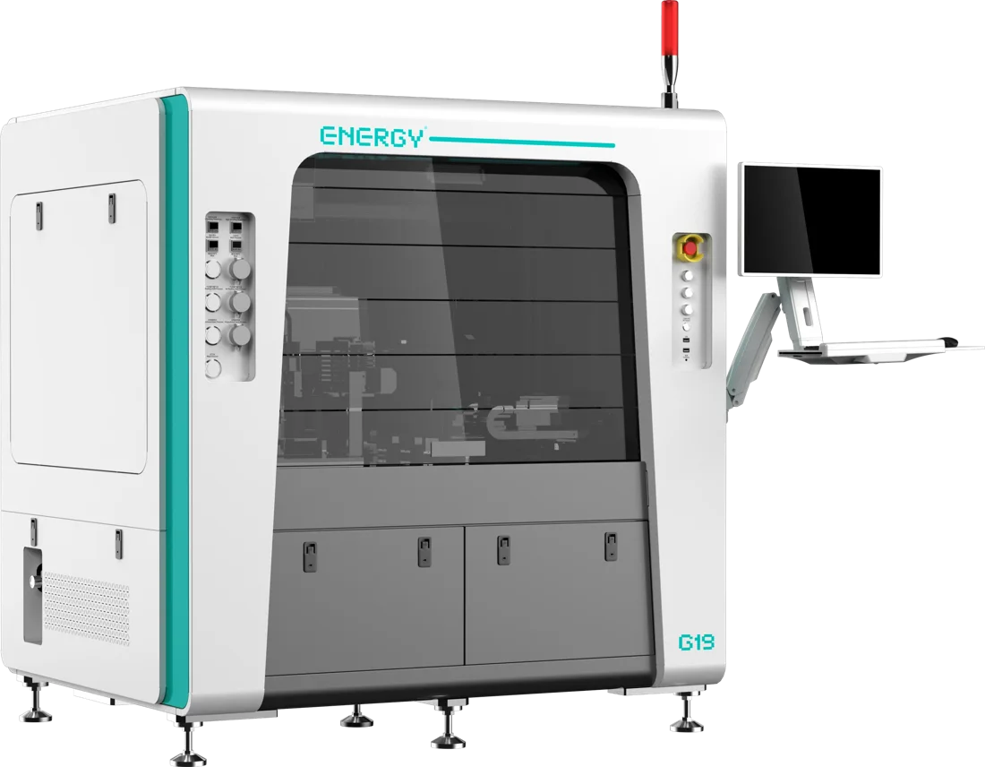
For epoxy or UV-cured COC and VCSEL placement at ±3 μm @3σ, see the G19 die bonder. Both machines are covered on the eutectic die bonder and optical module die bonder pages.
What this does not tell you
- The cited numbers come from different chip sizes and packages, so they are not interchangeable limits.
- Accuracy on a glass test die does not guarantee overhang on your parts.
- Void limits depend on your device and customer spec; agree them before the trial.