A MEMS sensor is a mechanical structure first and a chip second. Whatever the die attach does to the silicon, the sensing element feels it. Researchers describe die attach as the most important step in packaging high-precision MEMS sensors, because the bonding process itself typically induces thermal stress [1]. This guide pulls together what public papers say about that stress, and turns it into a checklist for choosing a die bonder.
Why die attach sets offset and drift
The package material usually has a larger coefficient of thermal expansion than the silicon or glass die. The two are fixed together at the adhesive cure temperature and then cool to room temperature, and the mismatch in shrinkage bends the assembly. In operation that warpage changes again with temperature, which shows up as drift [1].
The same paper notes that sensors with differential outputs, such as resonant accelerometers, are hit hardest by asymmetric stress, where one side of the die is bonded differently from the other [1]. A separate experimental and finite element study of a small 3.5 × 3.5 mm silicon die reports that most of the stress is generated during die attach, and that more compliant and thicker adhesives give great relief [4].
An adhesive supplier paper adds a distinction that matters for process planning. Stress locked in during assembly produces a zero offset that can be corrected. Stress from an adhesive that embrittles after repeated temperature cycling is irreversible and cannot be corrected out [3]. In that paper's tests, the larger stress input came from the cure step rather than from temperature changes in operation [3].
| Factor | What the sources say | Process lever | M18 Sense data point |
|---|---|---|---|
| Die handling | MEMS die must be handled from the chip sides so top-surface features are not damaged [2] | Membrane-safe pick and eject, no top-side contact | Membrane-protecting pick and eject |
| Adhesive stiffness | Silicones sit near 1 MPa, flexible epoxies near 100 MPa Young's modulus [3] | Choose the softest adhesive that still gives shear strength | Dot / write dispensing or dipping, adhesive set by you |
| Cure temperature | Stress builds as the bonded pair cools from cure temperature [1]; a supplier paper cites 150 °C standard versus 100 °C low-temperature cure [3] | Lower and shorter cure, tight oven control | Bonder places the die; cure is a separate step |
| Bond area and dots | Fewer, controlled dots cut stress, but dot-to-dot variation makes the stress asymmetric [1] | Repeatable dot volume and position, fixed bond force | Dot or write dispensing; voice-coil 20 to 50 g ±5 g, 50 to 200 g ±10% |
| Adhesive thickness | More compliant and thicker adhesive relieves die stress [4] | Hold a known bond line, avoid die tilt | Full seating of the die on the substrate after dispense |
| Placement | The die must land where the next step expects it, and a soft bond layer can let it move during ultrasonic wire bonding [2] | Placement accuracy plus a stable bond for wire bonding | ±10 μm @3σ XY with bottom camera (M18 platform) |
Bracketed numbers refer to the Sources list. Published values come from research papers and a supplier paper, so treat them as starting points for your own device. M18 Sense values are manufacturer specifications from the ENG product data.
Adhesive choice: flexible but not too soft
The supplier paper puts typical numbers on the trade-off. Highly flexible silicones sit around 1 MPa Young's modulus but give lower bond strength. Flexible epoxies sit around 100 MPa and bond harder but transmit more stress [3]. A low-modulus layer has its own risk: one packaging review warns that a low-modulus die attach can let the die move during ultrasonic wire bonding, which lowers wire bond strength, and that low-stress epoxies can be high-outgassing [2].
Low-stress adhesives in general have low modulus and cure at low temperature, but the 2019 study notes that polymer-based options can have poor bonding strength, which limits them where high reliability is needed [1]. So the adhesive and the wire bond process have to be chosen together. If you bond with aluminium or gold wedge wire next, check the bond force window with your wire bonder. The WB20 wedge wire bonder lists voice-coil bond force of 15 to 250 g ±0.5 g, Al wire from 17.5 to 75 μm, and a 63 × 63 μm minimum pad, so the same sample can be tested on both steps.
Dot pattern: fewer contact points, tighter control
One way to cut stress is to bond only part of the die. Attaching with a few adhesive dots reduces packaging stress and its variation, and several dots can still give a strong bond [1]. The catch is repeatability: the 2019 study cites another work showing that time-pressure dispensing varied by 9.7 to 36.5% in the same process, so the bonded area of each dot ends up different and the stress becomes asymmetric [1].
The authors' fix was a pillar on the die back side, where the adhesive fillet absorbs variation. They report shear strength above 35 N and incomplete fill and overflow of only 0.7% and 1.1% of the pillar area, with a final adhesive thickness of about 35 μm [1]. That is a die design choice made at wafer level, not something a bonder can add. For a bonder, the takeaway is simpler: dot volume, dot position and bond force must repeat from part to part, because those are the variables behind asymmetric stress.
Handling the membrane
Stress is not the only way die attach damages a MEMS part. The same packaging review points out that MEMS dies must be handled from the chip sides so top-surface features are not damaged, which rules out most standard pick-and-place fixtures [2]. Ejector needles that push through the tape can also crack thin membranes. For pressure and gravity sensors this is often the first thing to test in a trial run.
Where ENG equipment fits
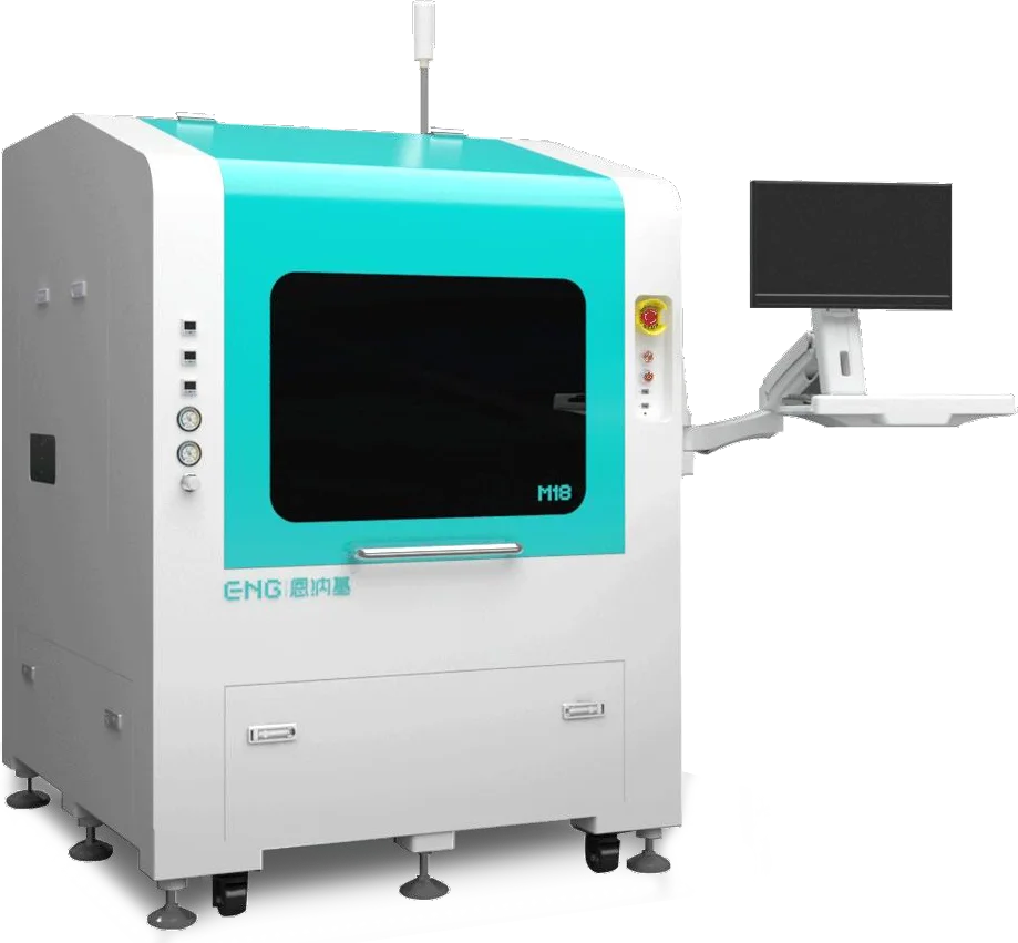
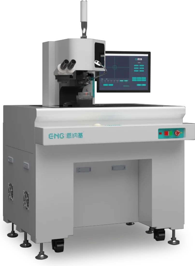
The M18 Sense sensor and TO die bonder is built around this handling problem. ENG lists membrane-protecting pick and eject, dot or write dispensing or dipping, and options for a bottom camera or pre-placement stage. Published specifications: XY accuracy ±38 μm @3σ, or ±10 μm @3σ with the bottom camera; 1,000 pcs/hr on an 8 in wafer with 0.8 × 0.8 mm die of 100 μm or thicker; die size 0.8 to 8 mm, with 8 to 30 mm custom; die thickness from 70 μm; voice-coil bond force 20 to 50 g ±5 g or 50 to 200 g ±10%; wafers up to 8 in on ring or frame. The M18-TO variant covers 0.2 to 5 mm die for TO headers and ceramic packages.
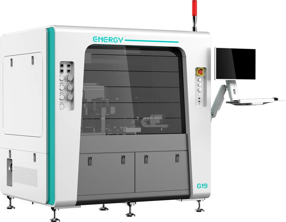
If your sensor die need tighter placement than that, the G19 high precision die bonder specifies ±3 μm @3σ XY. See the MEMS and sensor die attach page for how the machines map to pressure, gravity and inertial parts, or browse every application area.
ENG does not publish die stress or offset data for any adhesive. That depends on your die, package and cure, which is why we recommend measuring it on your own parts.
What we would not conclude from these sources
- The papers use specific devices (a resonant accelerometer, a 3.5 × 3.5 mm test die, microphones). Their numbers do not transfer directly to your sensor.
- The supplier paper is from 2012 and describes one supplier's adhesives. We cite it for the general trade-off, not to recommend a material.
- Nothing here says a particular bonder removes die stress. A bonder controls placement, force and dispense repeatability. The stress outcome also depends on adhesive, package and cure.
What to send for a MEMS sample evaluation
BondVane coordinates free sample bonding with ENG engineers. To make the trial useful, send:
- Die size, thickness, membrane or cavity location, and which side may be touched.
- Package or substrate (TO header, ceramic, LGA) and its surface finish.
- The adhesive you plan to use and its cure schedule, or the dot pattern you want to test.
- What you measure afterward: shear strength, offset, drift, or leak rate.
Use the sample evaluation form or the contact page to start.
Sources
- [1] An et al., Die-Attach Structure of Silicon-on-Glass MEMS Devices Considering Asymmetric Packaging Stress and Thermal Stress, Sensors 2019, 19(18), 3979
- [2] Eaton, Challenges in the Packaging of MEMS, Sandia National Laboratories, 1999
- [3] Koeniger, Highly Flexible Die Attach Adhesives for MEMS Packages, IMAPS International Symposium on Microelectronics, 2012
- [4] Walwadkar and Cho, Evaluation of Die Stress in MEMS Packaging: Experimental and Theoretical Approaches, IEEE Trans. Components and Packaging Technologies, 2006